
About Course
This course is about the Basic concepts of VLSI System Design.
The course is designed in the form of micro-videos, which deliver content in the form of Info-Graphics. It is designed for self-learning and will help to polish the Industrial skills. This course will cover the end-to-end description from basic Device Physics to Chip Design. The introductory video series focuses on the basic elemental physics and electrical characteristics of the MOS Transistor. Designing VLSIs is like building a city. Both jobs require significant forethought
All the best for your interviews and happy learning
Who this course is for:
- Individuals keen to learn about Chip World
Course Content
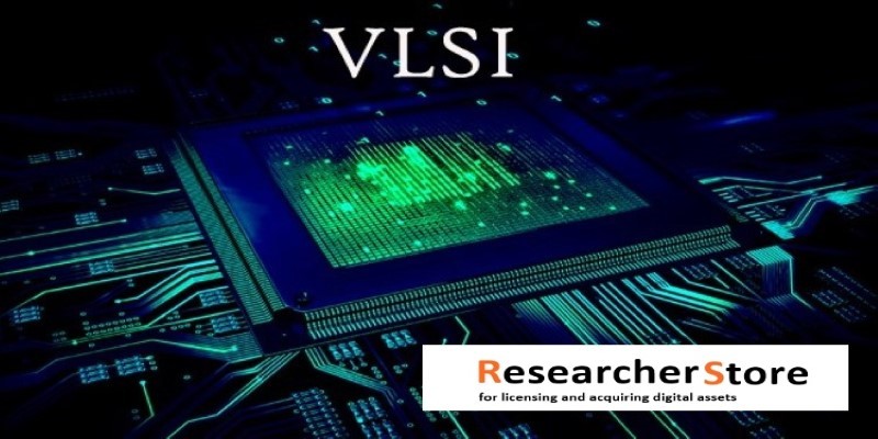
VLSI
-
Evolution of Logic Complexity in Integrated Circuit for Information Technology Services
00:00 -
VLSI design Methodologies
00:00 -
Comparison of Full Custom design and Semi Custom design
00:00 -
Semi Custom design in integrated circuit
00:00 -
Hierarchy, Regularity, Modularity and Locality
00:00 -
Package Technology in IC
00:00 -
VLSI design flow
00:00 -
Importance of CAD tools in VLSI design
00:00 -
Comparison of FPGA and CPLD
00:00 -
Comparison of FPGA, CPLD, PLC, Microprocessor, Microcontroller and DSP
00:00 -
CMOS Fabrication Process
00:00 -
Twin Tube CMOS Fabrication Process
00:00 -
Two terminal MOS and it’s Energy Band Diagram
00:00 -
Flat Band Voltage and Example on Flat Band Voltage
00:00 -
MOS under external bias
00:00 -
Thickness of Depletion Region, Depletion Region Charge Density & Surface Inversion in MOS structure
00:00 -
MOS Transistor, MOSFET
00:00 -
Threshold Voltage of MOSFET
00:00 -
Threshold Voltage Example
00:00 -
Gradual Channel Approximation in MOSFET, Drain Current Equation of MOSFET & MOSFET characteristics
00:00 -
Examples on Drain Current and Operating region in MOSFET
00:00 -
Channel Length Modulation in MOSFET
00:00 -
Substrate Bias Effect in MOSFET
00:00 -
MOSFET Capacitance
00:00 -
nMOS and pMOS basics, Symbol, Ideal Working, Input Characteristics & Output Characteristics
00:00 -
MOSFET regions of Operation with nMOS and pMOS
00:00 -
Examples based on nMOS and pMOS
00:00 -
pMOS and nMOS Comparison
00:00 -
Why is pMOS is good to pass logic 1 and nMOS is good to pass logic 0?
00:00 -
nMOS Inverter and Voltage Transfer Characteristics of nMOS Inverter
00:00 -
Noise Margin
00:00 -
Resistive Load Inverter
00:00 -
Example of Resistive Load Inverter
00:00 -
Depletion Load nMOS Inverter
00:00 -
CMOS Inverter
00:00 -
CMOS Inverter Voltage Transfer Characteristics
00:00 -
CMOS Inverter Parameters, VIH voltage, VIL Voltage and Noise Margin
00:00 -
Why pMOS size is greater then nMOS size?
00:00 -
Example on Symmetric CMOS Inverter
00:00 -
Example on CMOS Inverter
00:00 -
Examples of CMOS Inverter Voltage Transfer Characteristics
00:00 -
CMOS Inverter Examples
00:00 -
Propagation Delay of CMOS Inverter
00:00 -
CMOS logic circuit rules
00:00 -
CMOS NAND Gate (Basics, Circuit, Working and Truth Table)
00:00 -
CMOS NOR Gate (Basics, Circuit, Working and Truth Table)
00:00 -
Boolean Function Implementation using CMOS
00:00 -
CMOS Multiplexer (Basics, Circuit, Working and Truth Table)
00:00 -
CMOS Half Adder (Basics, Circuit, Working and Truth Table)
00:00 -
Boolean Function implementation using CMOS and equivalent size of CMOS Circuit
00:00 -
CMOS SR Latch using NOR Gates
00:00 -
CMOS SR Latch using NAND Gates
00:00 -
CMOS D Latch
00:00 -
CMOS SR Flip Flop using NOR Gates
00:00 -
CMOS JK Flip Flop using NOR Gates
00:00 -
Stick Diagram of CMOS NOR Gate
00:00 -
Stick Diagram of CMOS NAND Gate
00:00 -
Stick Diagram of Boolean Function
00:00 -
CMOS Transmission Gate and CMOS Transmission Gate as Tri State Buffer
00:00 -
Multiplexer Implementation using Transmission Gates
00:00 -
D Latch Implementation using Transmission Gate
00:00 -
Boolean Function Implementation using Transmission Gates
00:00 -
Dynamic CMOS
00:00 -
Cascading Issues of Dynamic CMOS
00:00 -
Comparison of Static and Dynamic CMOS
00:00 -
Domino Logic CMOS
00:00 -
Charge Sharing in Dynamic CMOS
00:00 -
Boolean Function Implementation using Dynamic CMOS
00:00 -
NORA CMOS Logic, NP CMOS Logic
00:00 -
Boolean Function Implementation using NORA CMOS Logic
00:00 -
Voltage Bootstrapping
00:00 -
Latch Up Problem in CMOS
00:00 -
Basics of clock and On Chip Clock generation
00:00 -
Ring Oscillator
00:00 -
Clock Distribution
00:00 -
BIST – Built In Self Test in Integrated Circuit
00:00
Student Ratings & Reviews

No Review Yet